Choosing a debug/programming connector for a microcontroller
TL;DR abstract: for ARM SWD, TI Spy-Bi-Wire, or Microchip ICD, use the Tag-Connect No-Legs footprint with standard pin/pad assignments, and get Tag-Connect cables.
When designing devices that use microcontrollers, one needs to provide a debug and programming connector. This might be used only for development, when writing and debugging software, or could also be left in production units, for in-factory programming.
Manufacturers and tool makers made sure that we live in a world where there is a multitude of debug connectors with lots of confusion around them. This is why we end up with this: 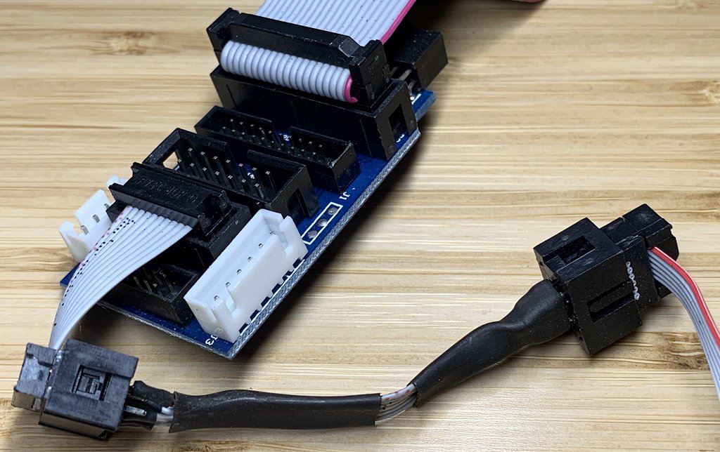
So, which connector to choose for a new design?
This article focuses mainly on ARM devices that have the SWD (Single-Wire Debug) interface, but it's also applicable to other parts, like Texas Instruments MSP430 which uses the Spy Bi-Wire (2-wire JTAG) protocol, Microchip ICD, or even parts that need a more complete set of JTAG pins.
Popular debugging connectors
Some of the common choices that are often considered:
- 10-pin JTAG on a 0.1" IDC header. Usually a male header is used. Disadvantage: it's huge, and the header costs money.
- Cortex Debug Connector using a 0.05" micro header (10-pin or 20-pin, Samtec FTSH-110 and FTSH-105). The 10-pin connector is reasonably small and available as an SMD part, but more expensive than IDC connectors.
- 20-pin 0.1" IDC connector. You are not seriously considering that dinosaur, are you? It's bigger than some of the boards I designed.
- Custom set of 4 or 6 pins (or vias, or copper pads). The problem here is the "custom" part. It will inevitably come back to bite you in the future, the day your custom connector breaks on the factory floor and you have to ship a new one from overseas, while production is halted.
- Tag-Connect 6-pin footprint in one of the variants (with legs or no-legs). Note that there is no connector here: just a standardized footprint on the PCB.
- Tag-Connect 6-pin + Tag-Connect 10 pin (for ETM signals): for this combination, there is even a pre-built cable available, with a 20-pin IDC connector and standard ARM Cortex 20-pin pin assignments.
One immediate observation is that most of these connectors require, well, connectors. That's an additional component that you need to place on the board, which costs money. For production units or larger prototype runs, that connector will only be used once in the entire lifetime of the product, which is a waste.
The Tag-Connect solutions or custom footprints with pogo-pin based connectors have an obvious advantage here in that they do not require any components to be placed on the PCB, so the debug connector per-board cost plummets down to 0, which is great!
This is how a Tag-Connect footprint looks like on a real board: 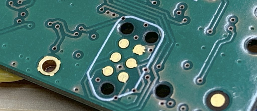
And this is what the cable with pogo-pins looks like: 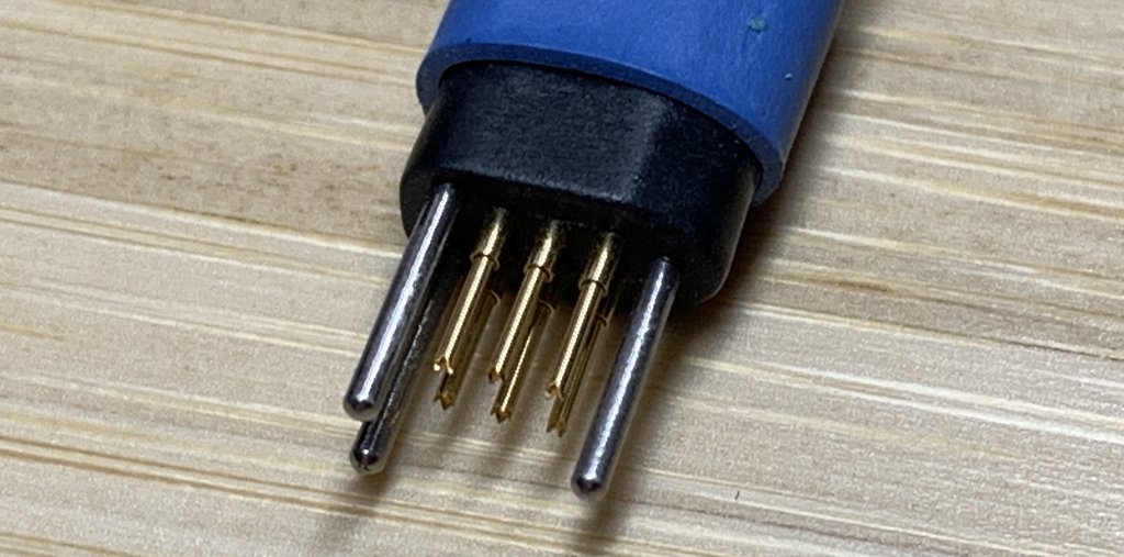 The second major consideration is size, and resulting board space requirements. The only contenders are the 10-pin 0.05" micro-header and a Tag-Connect 6-pin footprint. The 10-pin micro-header is actually a bit smaller in one direction, but the difference isn't significant. Here is what a 10-pin 0.05" micro-header looks like (this one is from a Nordic Semiconductor nRF52832 development board, the PCA10040):
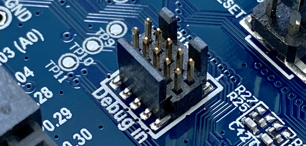
Legs or No-Legs?
There are two variants of a Tag-Connect connector cable: one with "legs" and one with "no legs". What's the difference?
Tag-Connect uses pogo pins, which have springs inside and push against the PCB. If you want the connector to stay in place, you have to continuously apply force to it. This is fine for quick programming, where you can use one hand to hold the connector in place and another to launch that programming job, but does not work that well for extended debugging sessions. For that, the "legs" footprint (and connector) works much better. The legs act as little clips, so once you insert the connector, they snap into place and hold the pogo pins tight against the board, for an indefinite time.
The problem with the "legs" footprint is its size: it is significantly larger than the "no-legs" variant. What's worse, it needs four large holes in the board. Large holes are always a problem: they (obviously) need to pass through all layers, and you need a keepout area around them as well. This means that the impact of a "legs" footprint on your design is much bigger than of the "no legs" variant.
For production units, where the connection will likely only be made once in the lifetime of a product, and can easily be hand-held all the time, there is no question: you definitely prefer the "no-legs" footprint, which saves board space. But what to do about the prototypes? On one hand, you can afford the board space, but on the other hand, you do not want to redesign the PCB just because you need to remove the holes in the final revision.
Luckily, there is another solution. Tag-Connect sells a little retaining clip. It's a piece of PCB with three sockets that fit the pins of the Tag-Connect cable. It's not a mechanically perfect solution and the clips tend to wear out with time (they are also incredibly easy to lose!), but in practice it works quite well.
My recommendation is to always go with the "no-legs" footprint and cables, buy a bunch of retaining clips, and save on board space and redesigning the boards.
Use a standard signal assignment
I've seen hardware in the wild, where designers used a Tag-Connect footprint for ARM SWD (on a Cortex-M0), but assigned signals differently. It's likely the motivation was to obfuscate the interface.
This is not something I'd recommend: the obfuscation is easily discovered, and one ends up with an incompatible footprint, which will inevitably cause trouble in the future.
Practicalities
Tag-Connect recommends that no components be placed (or traces routed) on the other side of the footprint. While that is a good recommendation, one does not always have that luxury, especially on small boards with tight layout constraints.
As I've discovered, you can get away with placing components on the other side, even when you use the retaining clip to hold the cable in place. I would suggest using a piece of insulator between the components and the retaining clip, though, to prevent any possible shorts (paper works well). While not the recommended practice, this does work, although fixing the debug connector in place gets a bit more involved.
Here is an example of a prototype board (please excuse the prototype solder quality) where components are placed within the area of the debug footprint: 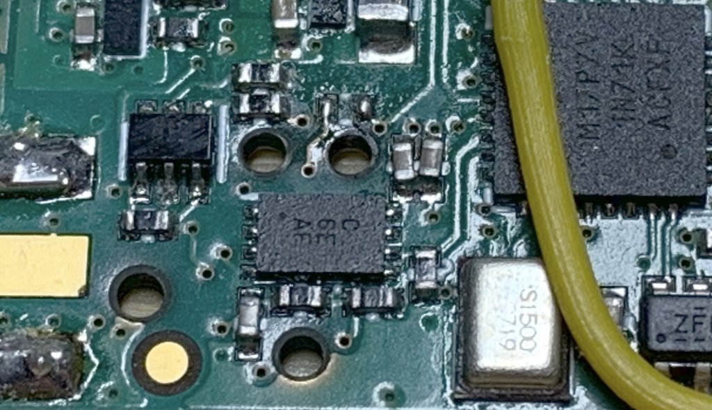
Criticism
It's not all roses with Tag-Connect. The website is not well organized, so it's difficult to find the information you're looking for. There is a multitude of variants offered, and even though most people will need a single type of cable, it isn't prominently displayed. Unfortunately, this seems to be a tradition with companies making debug and programming equipment in the embedded world.
The second gripe I have is that the company offers downloadable CAD libraries with Tag-Connect footprints, but states that:
These files are provided 'AS IS' and with no guarantee that they are complete, free from errors or suitable for use. Carefully check the imported decals against the latest datasheet provided on the Tag-Connect website (see below). In particular pay check hole sizes, pin numbering, and pay close attention to the solder paste-mask layer to ensure no solder paste is deposited on the footprint pads.
If you look in the ZIP files provided, there will usually be several footprint variants for a given CAD. Which one do I use? And why is it my responsibility to verify it?
I think Tag-Connect should clean up this library and provide a set of supported footprints, at least for the more popular CAD packages, without a disclaimer. It should be part of the value of this solution.
Conclusion
All things considered, Tag-Connect is still the best off-the-shelf debugging and programming solution. I'd recommend standardizing on it and using it in all your designs.
Earlier blog posts: KiCon 2019 (2019-03-27)
Later blog posts: What's new: May 2020 (2020-05-16)
PartsBox is an online app that lets you take control of your electronic parts inventory, BOM pricing, and small-scale production. It keeps track of where components are stored, what the current stock levels are, and which components are used in which projects/BOMs.
Blog Index
Quick tip: part spec overrides (2026-03-27)
What's new: early 2026 (2026-02-08)
2025: A Year in Retrospect (2026-01-14)
Use your parts library in KiCad (2025-05-12)
Improved BOM Management (2025-03-01)
Building Rockets: Aerospace Team Graz (2024-02-13)
Building Satellites with PartsBox: A Case Study (2023-12-01)
Images for parts, locations and projects (2021-01-27)
Heads-up: changes in builds ⚡️ (2021-01-12)
October 2020 update (2020-10-12)
What's new: May 2020 (2020-05-16)
KiCon 2019 (2019-03-27)
2018: A Year in Retrospect (2019-03-22)
2017: A Year in Retrospect (2018-01-09)
Barcode scanner support (2017-06-18)
Resources for hardware startups (2017-05-19)
How to organize electronic parts (2017-05-07)
BOM Pricing for projects is now available (2017-05-05)
Tags (2016-04-26)
Projects (BOM management) (2016-04-20)
An improved search engine (2016-02-27)